Дом с отличной планировкой в Динской | Длительность: 9:29 | Просмотры: 1.5K


In a fabricating process for a small DRAM such as a 60 nm DRAM, it is essential to form a buried word line in order to increase the integration degree of a transistor in a cell, simplify a. 16 дек. 2021 г. · In our example, wordline recess depth and etch selectivity (to active area silicon) have the greatest effect on wordline resistance (figure 5), and they can be adjusted until a targeted … 23 февр. 2022 г. · With the solutions pro-vided by the examples of the disclosure, damage to the semiconductor substrate can be avoided, and the man-ufacturing process of the buried word line … 3 апр. 2019 г. · As dynamic random access memory (DRAM) scales to 20 nm and sub-20 nm, titanium nitride (TiN) recess with selectivity to tungsten (W) becomes one of the key process for fabricating … 3 янв. 2023 г. · In a buried word line (bWL) device, a word line is buried below the surface of a semiconductor substrate using a metal as a gate electrode. The selection of metal to be used as a … The present disclosure relates to a semiconductor device having a buried word line and a method of manufacturing the same, and more particularly, to a recessed access device (RAD) transistor and a … 3 апр. 2019 г. · As dynamic random access memory (DRAM) scales to 20 nm and sub-20 nm, titanium nitride (TiN) recess with selectivity to tungsten (W) becomes one of the key process for fabricating … In DRAM buried wordline (bWL) cell (also refer to page4838), the transistor gates are merged with the metal WL running below the silicon surface level, resulting in a simple cell structure. Methods for DRAM device with a buried word line are described. The method includes forming a metal cap layer and a molybdenum conductor layer in a feature on a substrate. We demonstrate high array device on-current, small parameter variability, high reliability and small parasitic capacitances, resulting in an excellent array performance. The array device can be scaled …
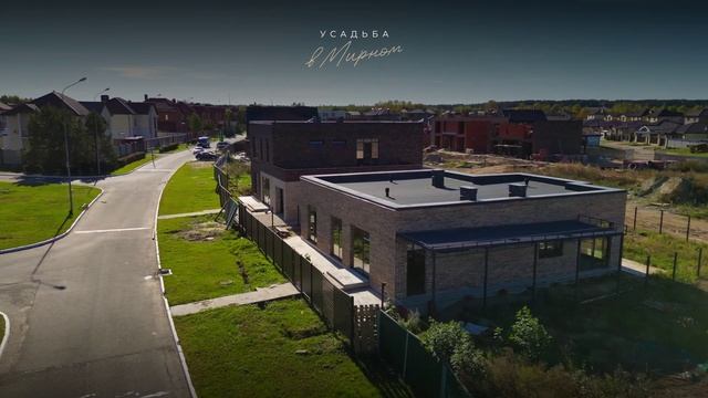
🏡ID 70289878 Для связи со мной: 📲 Телефон +7 (928) 211-33-77 Наш телеграм канал с домами и ценами, а так же актуальной инфо...
Автор: Переезд в Краснодар | Просмотров: 1.5K | Длительность: 9:29


Ситуация на рынке вторичной недвижимости в частном секторе станицы Динская Красн...
23:07
102
Бойкая Семейка